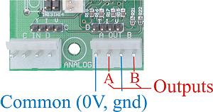
The above picture shows the connections for the two external analog outputs. They are designated analog outputs A and B. Each output can generate a 0-10V signal, with a maximum load current of 5mA, corresponding to a 2KOhm load. The outputs have internal current limiting (which is not the same as being short circuit proof!).
The analog output voltage is a positive voltage measured with respect to the 0V terminal. It is programmed using the AnOutA or AnOutB instruction. With X=0 this will result in 0V out, with X=255 it will result in 10V out.
The output resolution is 8 bits (256 steps between 0 and full scale) when you use the AnOut# instructions and 10 bits when you use fAnOut. The output is generated as a filtered pulse width modulated (PWM) signal. The filter consists of a simple 100mS RC low pass filter. For a full scale step output change, say from 0V to 10V, this will take 230mS to settle to within 10% of the full change, 450mS to settle to 1% and 550mS to settle to 0.4%.
NOTE: In the MMi200 the OBCA cannot be used in the same program as Analog outputs A and B. If you attempt to do so you will get a runtime error. Analog outputs I and J (thermistor drive and SPice connector) are not affected.
This does not affect the MMi99, MMi201 or MMi203.
Here are some ways of blowing up the analog outputs: